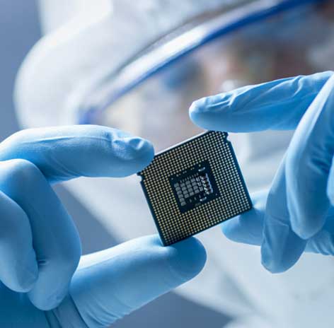
CMOS (Complementary Metal Oxide Semiconductor) image sensors are found in most cameras and cell phones today. These image sensors use silicon as the photon absorption layer and employ state-of-the-art device and process technology to produce sensors with high sensitivity and low noise. Quantum Semiconductor’s image sensors use Group-IV superlattices, for example SiGeC, for the photon absorption layer to provide increased sensitivity, through the higher efficiency of light absorption afforded by Group-IV superlattices.
Group-IV superlattices also enable detection of wavelengths beyond the visible spectrum, for instance in the infra-red, which can help with imaging in low light conditions. Image capture can also be improved with noiseless amplification which is a special feature of the Quantum Semiconductor photodiode.
Quantum Semiconductor photodiodes and Group IV superlattices can be manufactured using standard Si wafers with conventional CMOS fabrication tools, and therefore benefit from the economies of scale that silicon-based manufacturing brings to the microelectronics industry.

Silicon photonics uses the optical properties of silicon, a group-IV semiconductor, for the design and fabrication of devices to manipulate and detect light. Silicon is a great absorber of light but its indirect band structure means that it is does not create light.
Quantum Semiconductor LLC has been investigating Group-IV superlattices to enable the absorption and emission of light in the Short-Wavelength Infra-Red (SWIR) range, including 1.55µm and longer wavelengths. Many of the compositions which have been discovered have direct band gaps, making it possible to have efficient light emission from emitters monolithically integrated with CMOS, without additional discrete or heterogeneously integrated components. The lower parasitic capacitance of monolithic integration makes it the ideal solution for silicon photonics with higher speed and lower power dissipation. Some superlattices can absorb or emit light selectively along certain directions, while others have similar properties for all directions.

Light Detection And Ranging, or LiDAR, uses light to measure distances, similar to how RADAR uses radio waves. LiDAR technology measures the distance between objects by hitting the target with a laser and analyzing the reflected light. The 3D image formed by the receiving sensor is called a point cloud.
LiDAR has many applications including in agriculture, astronomy, atmospheric and geospatial mapping and research. Perhaps the most important future application is in self-driving, or autonomous vehicles, where LiDAR can be used for navigation, collision avoidance and for autonomous cruise control in adaptive cruise control (ACC) systems.
The level of accuracy of a LiDAR system can vary depending on the power, configuration and resolution of the unit. Single-photon detection is the ultimate sensitivity which can be used for light-sensing and is particularly useful for LiDAR systems because it allows the system to see farther and to detect objects more quickly. The noiseless gain of Quantum Semiconductor photodiodes can provide this extreme sensitivity in the sensors. Coupled with the use of Group IV superlattices as the sensor materials, Quantum Semiconductor sensors can be used with Short-Wavelength Infra-Red (SWIR) range lasers around the 1.55µm wavelength, which is ideal to provide eye-safe operation.
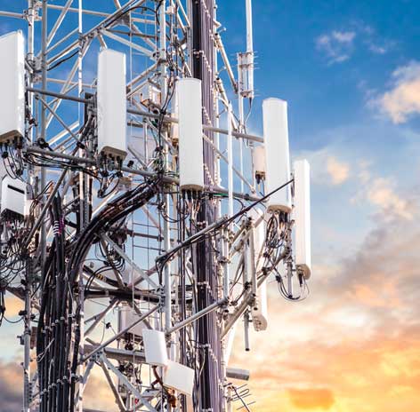
Broadband high-data rate services and wireless telecommunication standards require high-performance devices operating at ever higher frequencies with reduced power consumption. BiCMOS combines two different device technologies, Bipolar and CMOS, into a single chip for optimum performance. The Bipolar transistors result in high speed and gain, which are critical for high-frequency analog applications, and CMOS technology is used for high-density and low-power logic gates. The heterojunction bipolar transistor (HBT) is a type of bipolar junction transistor (BJT) which uses differing semiconductor materials for the emitter and base regions, creating a heterojunction. The HBT improves on the Bipolar Junction Transistor (BJT) in that it can handle signals of very high frequencies, up to several hundred GHz.
BiCMOS uses SiGe technology in the Heterojunction Bipolar Transistors (HBTs) to improve high-frequency performance and reduce the power consumption. Typically, a small percentage of Carbon is present in the SiGe layers to compensate strain in the film. Replacing these SiGe or SiGeC random alloy films with Quantum Semiconductor’s Group-IV superlattices in the BiCMOS HBTs Base layer, and/or Emitter and/or Collector layers, enables superior electron and hole transport speed, resulting in better performance at higher frequencies of the wireless spectrum. These Group-IV superlattices also enable the co-fabrication of speed-optimized Complementary HBTs, which is very desirable for analog and mixed-signal design for high-frequency wireless applications. Complementary HBTs are not possible with SiGe or SiGeC random alloys due to the lack of suitable band offsets to design PNP-HBTs.
In addition to telecommunications, other applications include automotive, defense, security, scientific instrumentation and satellites.

Quantum computing uses quantum bits, or qubits, for computation in place of the standard bit which typically is implemented in a silicon microprocessor. There are many ways to make physical qubits, such as the spin up or down of electrons.
Quantum Semiconductor LLC has been working to discover Group-IV superlattices which have direct bandgaps and interesting properties. Some Group-IV superlattices have been found to have Topological Properties which provide unique light-matter interaction through second order optical effects and spin engineering. These materials could be used to make physical qubits. What makes these materials so attractive is that these superlattices can be monolithically integrated with conventional CMOS and can be key building blocks for novel quantum devices.

Random numbers are useful for a variety of purposes, such as generating data encryption keys, simulating and modeling complex phenomena and for selecting random samples from larger data sets. A random number is one that is drawn from a set of possible values, each of which is equally probable. In a sequence of random numbers, each number is statistically independent of the others. The occurrence of random physical phenomena can provide a basis for true random number generation, as opposed to using an algorithm on a computer to generate pseudo-random numbers. The problem with physical random number generators is that they tend to be slow.
Random phenomena that occur in electrical circuits can be used to generate random numbers. In the Quantum Semiconductor photodiode, random shot noise in the photo-generated signal appears when light intensity is very weak. This also makes the electronic signal very weak, which cause electronic circuits to be slow. On the other hand, it is desirable to have the highest possible rate of random number generation. The noiseless gain in SiGeC photodiodes can be used to provide a very large amplification of the shot noise signal, thereby ensuring much faster circuit operation, which is critical for mass encryption and hand-off.